Products
Product Examples
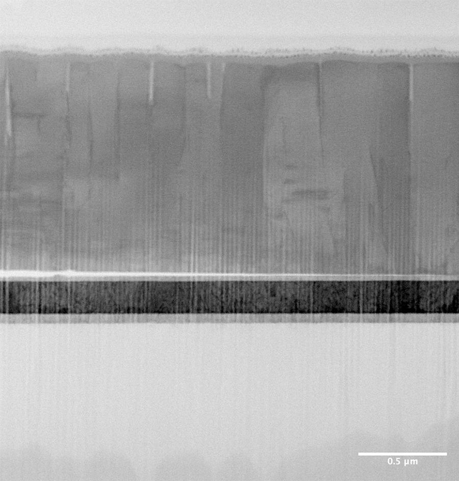
Scanning transmission electron microscope (STEM)
Observation of fine structures that cannot be observed with optical microscopes by using electron beams, which have shorter wavelengths than light.
The internal structure is observed by detecting electron beams transmitted through a thin sample.
Uniform high-quality single-crystal lattice images.
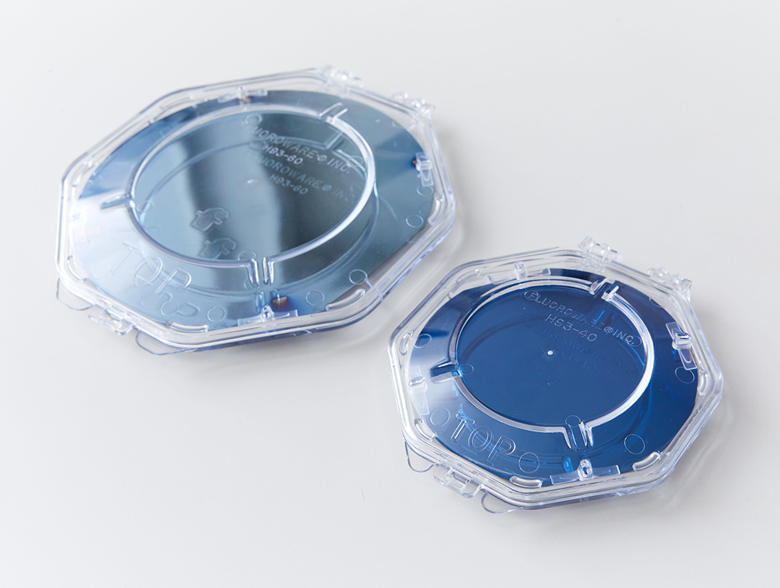
6inch/4inch high quality single crystal film
Capable of providing a wide variety of high-quality single-crystal thin films such as PZT/SiC/GaN.
The company target to larger-diameter production to 12-inch diameter with its proprietary “M4” technology, which has evolved the platform from the laboratory level to the mass-production level.
The major feature of Gaianixx PZT thin-film is that the dielectric constant is about 100 to 450 (phase boundary) and polarization is completed at the end of deposition, so spontaneous piezoelectricity™ is maintained. In addition, it has high heat resistance and does not depolarize even at 450°C (reflow temperature).
Core Technology
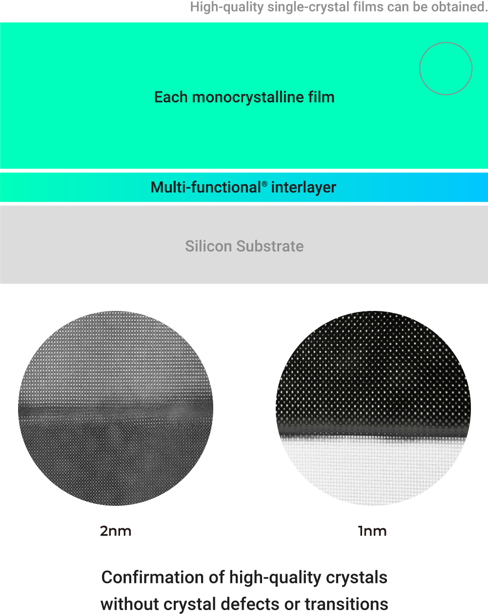
“Multi-functional® interlayer”, which enables high-quality single crystals in a multilayer structure.
By forming a “Multi-functional® interlayer” on the substrate, the lattice constants of the substrate will matched to first layer and form a single crystal layer.
The greatest feature is not only the first layer, but also the detects the stress of multiple material and layers grown on top of first layer, which again reforms arbitrarily by “Dynamic lattice matching” to form high quality single crystals on multiple layers.
This is because Gaianixx’s multifunctional interlayer causes the top functional film to become monocrystalline by creating dynamic lattice matching through twinned martensitic transformations driven by lattice mismatches.
Also “Multi-functional® interlayer” are possible to grow high-quality single crystals without affects of defects on the substrate, which is expected to contribute significantly to yield and cost improvement.
Predominance
Point1
High Quality
Point2
High Performance
Point3
Miniaturization
Mechanism
Dynamic Lattice Matching
Crystallinity
Single-Crystal Ultra Thin Film
Characteristic
Pauling-less polarization
Assessment Results
Evaluation Result with Gaianixx PZT
Thermal resistance
(Tc)
600℃
Voltage resistance
(/μm)
200V
Piezoelectric constant
(d31:pm/v)
250
Hysteresis characteristics/Curve

“Multi-functional® interlayer”
Remarkable performance improvement in
crystalline piezoelectric films
Comparison of other companies’ piezoelectric characteristics
2x
Displacement
value
2x
Thermal
resistance
7x
Voltage
resistance
Equipment and Quality Control
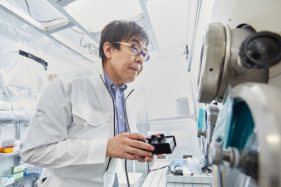
Ceramics formation technology using our unique dual-frequency inductively coupled plasma type physical vapor deposition system
We are working on the establishment of an absolute theory for dual-frequency inductively coupled radio-frequency plasma-based ceramics deposition (ICPVD) in collaboration with the University of Tokyo, and at the same time, we are working on AI of the basic theory for the establishment of mass production technology for 8-inch wafers.
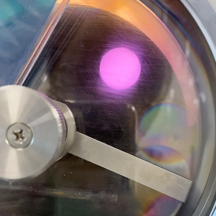
ICP plasma phenomena during “Multi-functional® interlayer” film formation
We most focused on the specific impact of the dual-frequency ICP plasma phenomenon on device characteristics using its ceramics thin films, as a set value for the preparation of ceramics thin films.
Environmental Initiatives and Policies

- Social value created by single-crystal semiconductor films
- We develop and manufacture single-crystal films, which are indispensable for realizing high value-added, compact, and low-cost semiconductors such as MEMS, power devices, and LED products, using the world’s only Multi-functional® interlayer film, and create value for society in the mid- to long-term with our partners.
- Value Creation Platform
- Establish a manufacturing technology platform for various compound semiconductor single-crystal films based on the established “M4” (Material, Machine, Method, Member) technology and step up from the laboratory level to mass production scale.